
Samsung’s LPDDR5X-PIM Breakthrough: Redefining AI Inference at Hot Chips 2026
Executive Overview
The artificial intelligence hardware landscape is undergoing a monumental reckoning, driven not by a lack of raw processing power, but by the physical limits of memory bandwidth and the exorbitant costs associated with high-end memory architectures. At the prestigious Hot Chips 2026 conference, Samsung Electronics took center stage to showcase a transformative development that could recalibrate the economics and performance of edge AI: the industry’s first fully validated LPDDR5X-PIM (Processing-in-Memory) standard.
By integrating specialized computing logic directly into low-power dynamic random-access memory (DRAM) cells, Samsung is shattering the traditional "von Neumann bottleneck"—the sluggish data transit corridor that forces processors to endlessly wait for data to travel back and forth from memory banks. According to preliminary benchmarks and technical deep-dives presented at the conference, Samsung’s new LPDDR5X-PIM architecture achieves a staggering 2.28x improvement in model run time and a 3.01x boost in tokens per second (TPS) during large language model (LLM) inference tasks, all while maintaining a power envelope comparable to conventional memory modules.
This comprehensive overview examines the architectural triumphs, technical specifications, and profound market implications of Samsung’s Processing-in-Memory initiative, charting a course toward a future where efficient AI acceleration moves out of hyper-expensive data center server racks and directly into client devices, mobile ecosystems, and power-constrained edge accelerators.

Detailed Chronology and Technical Evolution of PIM
Processing-in-Memory is not an overnight revelation; rather, it is the culmination of nearly a decade of research and iterative engineering by memory heavyweights looking for a way around stalling CPU and GPU scaling.
The Origins of PIM (2021–2023)
Samsung first teased the concept of Processing-in-Memory back in 2021, initially piloting the technology through High Bandwidth Memory (HBM) stacks integrated into modified AMD MI100 accelerator GPUs. While HBM-PIM proved that performing basic arithmetic operations locally within the memory stack could dramatically accelerate massively parallel workloads, it suffered from a fundamental commercial drawback: HBM remains prohibitively expensive.
By 2023, Samsung had formalized the HBM-PIM concept into a commercial roadmap and simultaneously introduced the theoretical groundwork for LPDDR5X-PIM. However, these early disclosures were strictly conceptual. The milestone presented at Hot Chips 2026 marks the critical transition from theoretical whitepapers to silicon-validated, production-ready hardware undergoing rigorous real-world testing.

Moving Beyond HBM: Why LPDDR5X?
The race to integrate PIM into the LPDDR5X standard is fueled by mounting economic pressures within the semiconductor supply chain. During the Hot Chips conference, rival memory manufacturer Micron warned that the silicon gap and wafer demand disparity between HBM and conventional DDR5 are widening exponentially with every new hardware generation. Memory now constitutes the single largest component cost in modern AI accelerators, and that financial slice is expanding.
While HBM delivers phenomenal data throughput, its high manufacturing complexity and cost relegate it primarily to top-tier enterprise data center accelerators (such as NVIDIA’s H100, B200, and their successors). By contrast, LPDDR5X has traditionally served mobile devices, laptops, and thin-and-light form factors. By grafting PIM architecture onto LPDDR5X, Samsung is effectively democratizing in-memory computing, bringing server-grade acceleration efficiencies down to the client and edge hardware tiers.
Architectural Deep-Dive: How LPDDR5X-PIM Works
To fully appreciate the engineering feat achieved by Samsung’s hardware teams, one must examine how logic gates are shoehorned into delicate DRAM arrays without compromising stability, density, or power efficiency.
1. Bank-Level Integration and the MAC Tree
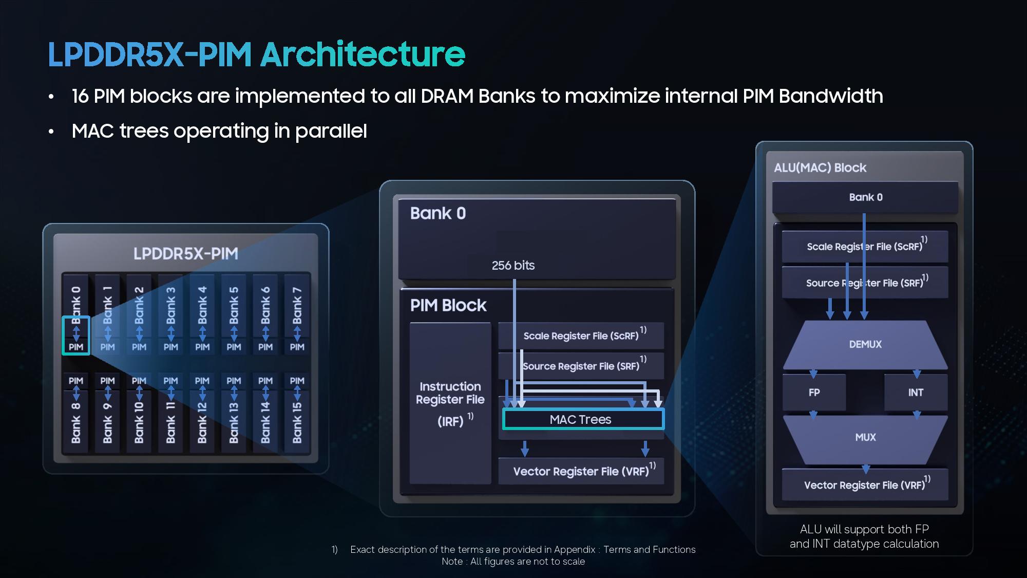
In previous iterations like HBM-PIM, engineers were forced to completely sacrifice entire memory banks to make physical room for the auxiliary processing logic. Samsung’s LPDDR5X-PIM architecture circumvents this limitation through refined die layouts.
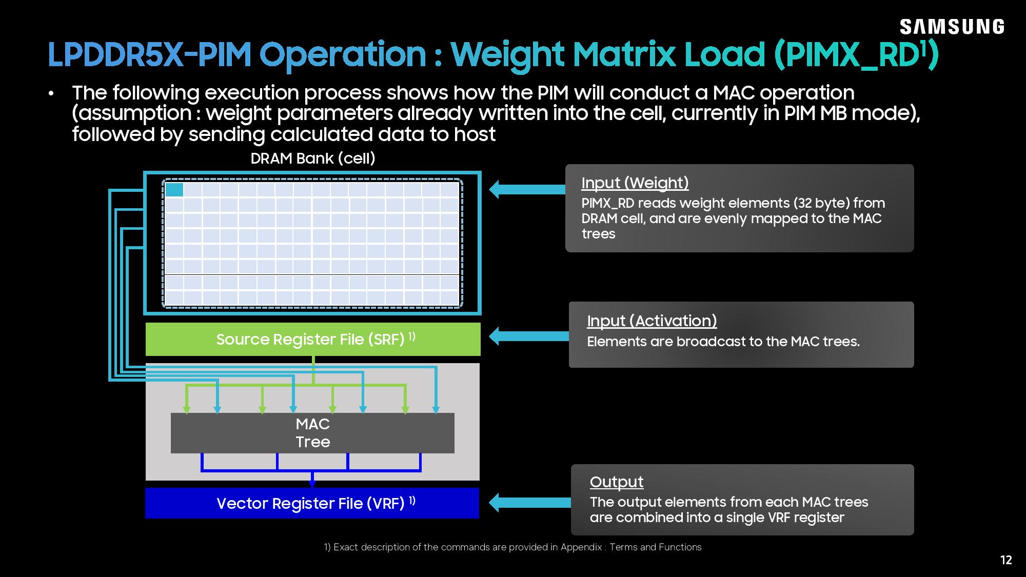
In the new LPDDR5X-PIM design, every individual memory bank houses its own dedicated PIM logic unit. As data flows out of the memory cells, it interacts with a scale register file and a source register file, both of which feed directly into parallel Multiply-Accumulate (MAC) trees. These MAC trees perform the heavy lifting of matrix multiplications—the core mathematical operation underpinning all neural network inference—locally within the chip. Once the calculations are computed, the final integer or floating-point output values are safely stored in a specialized Vector Register File (VRF).
2. Dual-Mode Operation and Address Align Mode (AAM)
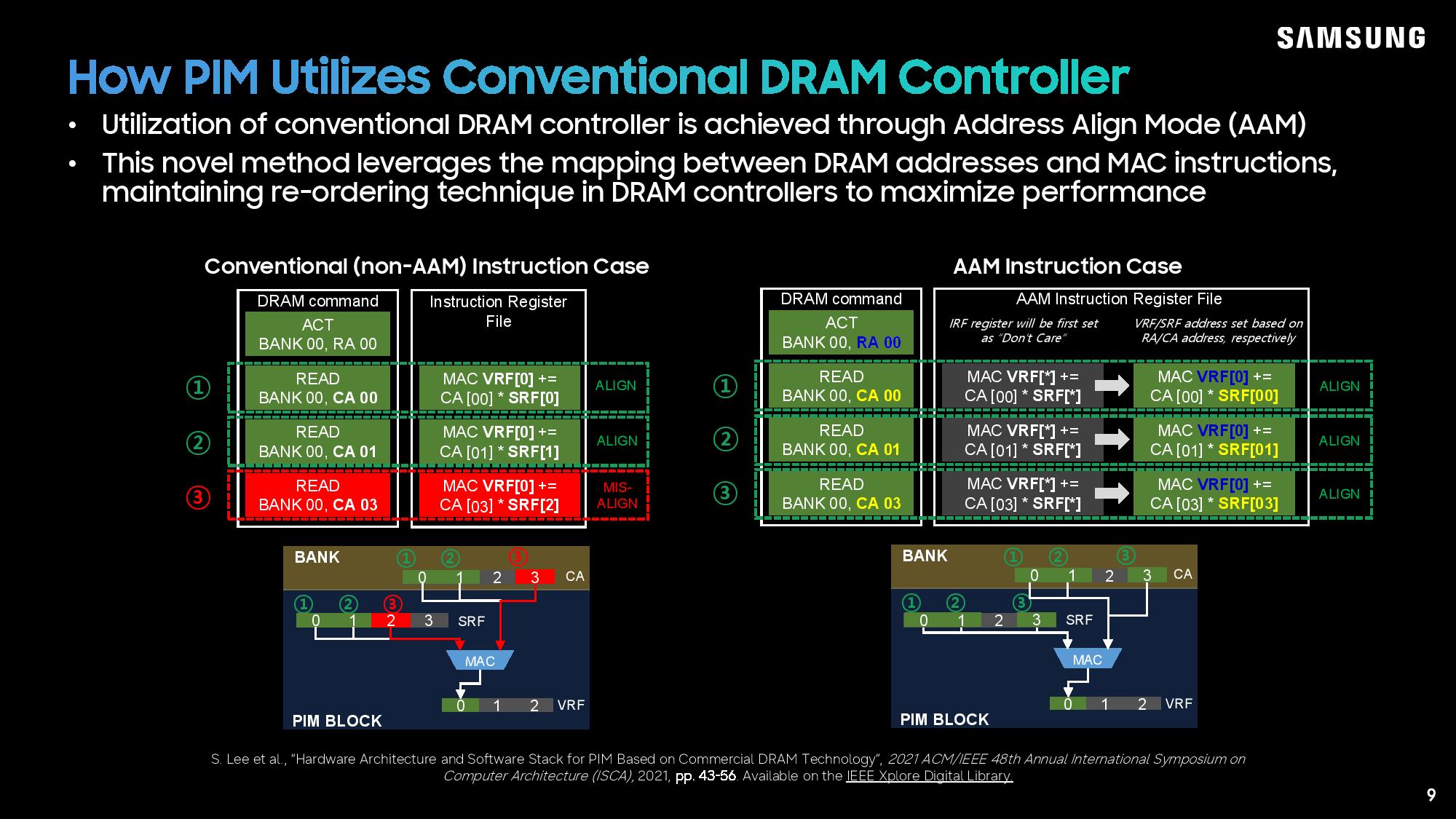
Integrating compute logic into standard memory introduces a massive scheduling challenge: how do you prevent conventional memory controllers from breaking when instructions are reordered?
Samsung solved this hurdle by designing LPDDR5X-PIM with two distinct operational modes:
- Single-Bank Mode: Functions identically to traditional, legacy DRAM, allowing seamless, standard read and write operations.
- Multi-Bank Mode: Activates the PIM logic, transforming standard memory channels into localized compute engines.
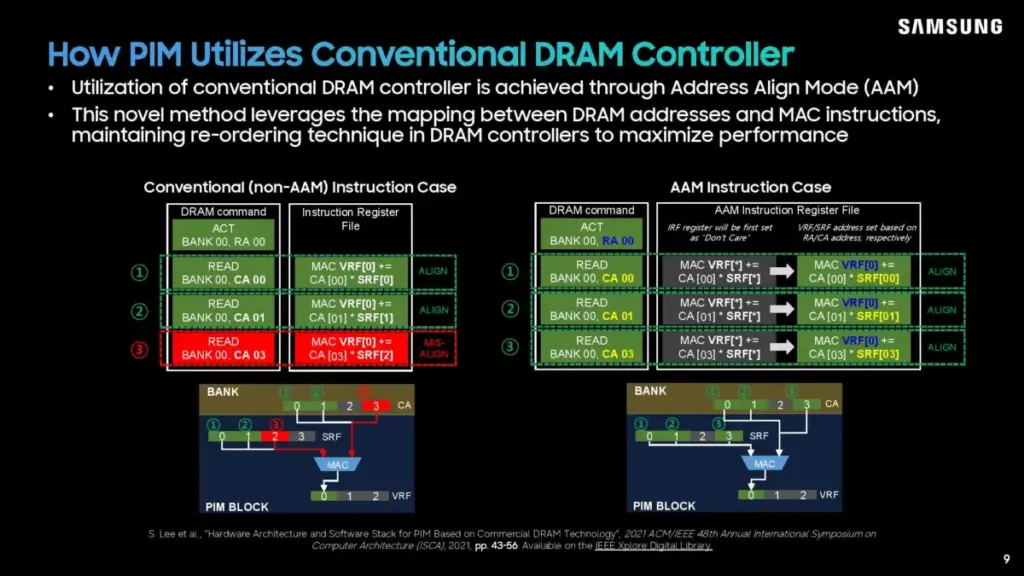
Because conventional memory controllers struggle with the instruction reordering required during PIM computations, Samsung developed Address Align Mode (AAM). AAM cleverly maps standard DRAM addresses directly to MAC instructions. Instead of relying on a complex Instruction Register File that could disrupt scheduling, AAM assigns Vector Register File (VRF) and Source Register File (SRF) addresses dynamically based on Row Address (RA) and Column Address (CA) coordinates.
3. Step-by-Step Data Flow Example
To illustrate this intricate dance of data, Samsung outlined a typical FP8 (8-bit floating-point) activation data processing cycle during its Hot Chips presentation:
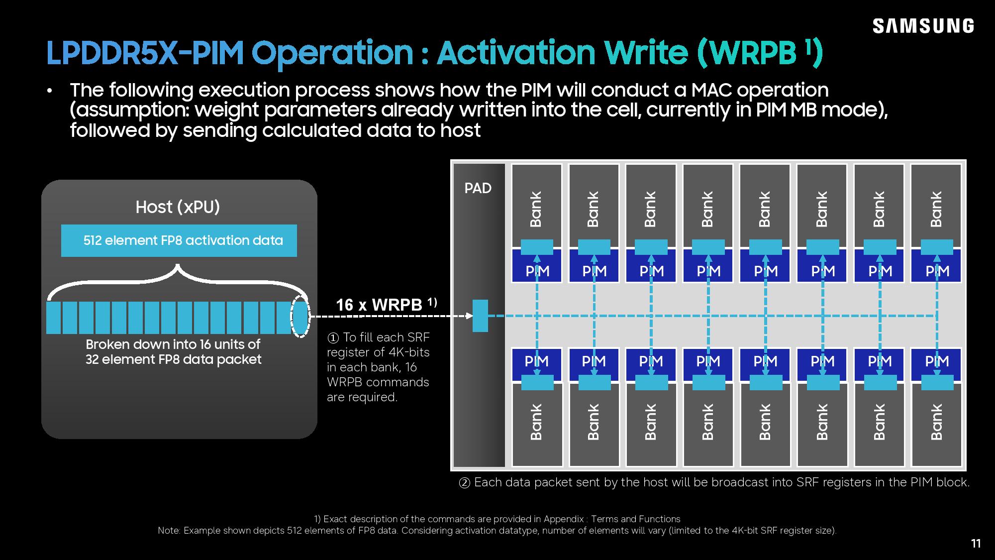
- Data Ingestion: A 512-byte block of FP8 activation data is broken down into sixteen 256-bit packets, which are written into individual memory banks and cataloged within the Source Register File.
- Local Execution: A specialized
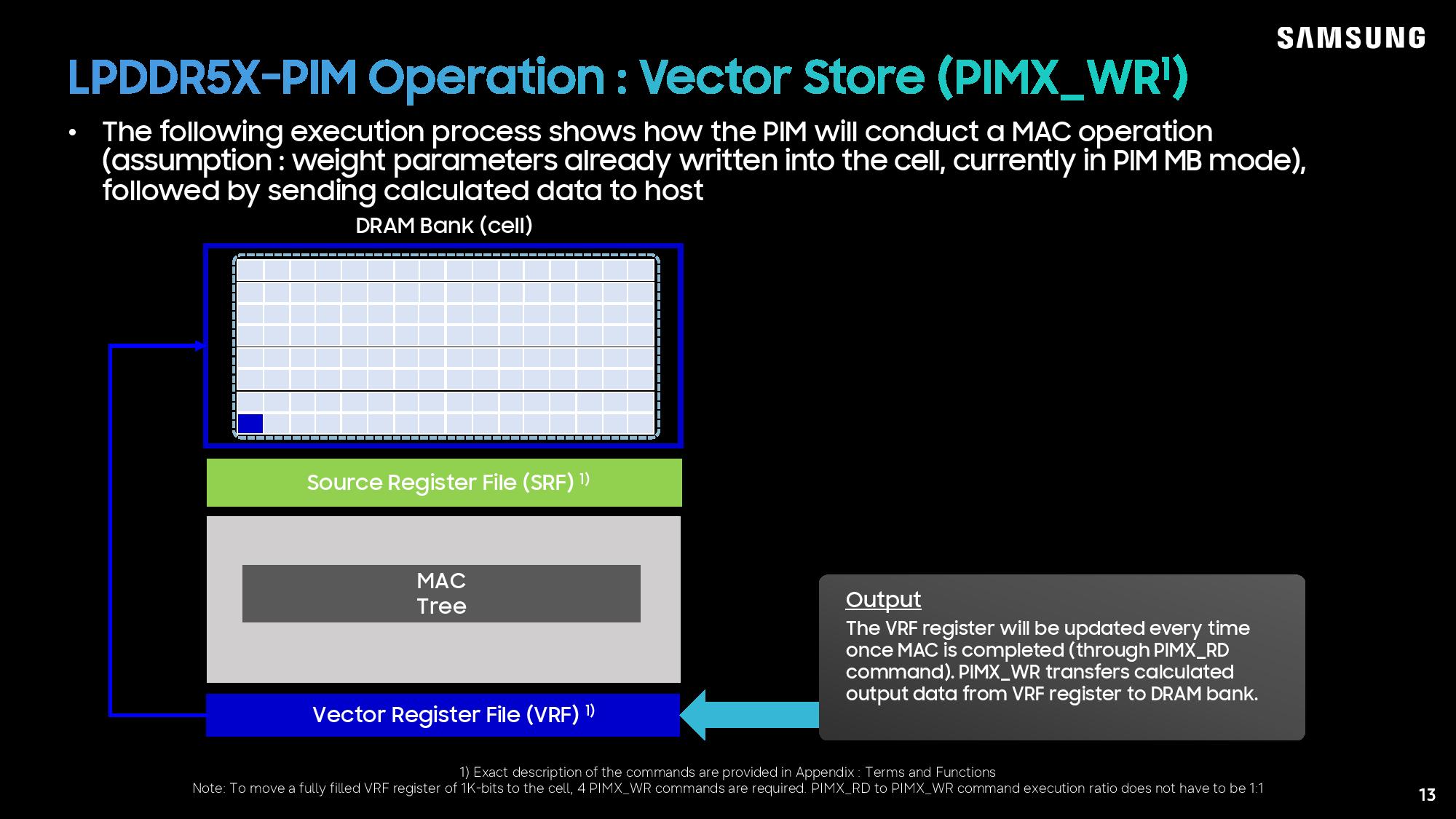
PIMX_RDcommand pulls pre-loaded weight parameters out of the DRAM bank, routing them directly into the parallel MAC trees alongside the activation data waiting in the SRF. - Vector Storage: The resulting output vectors from the localized calculations are immediately written to the Vector Register File.
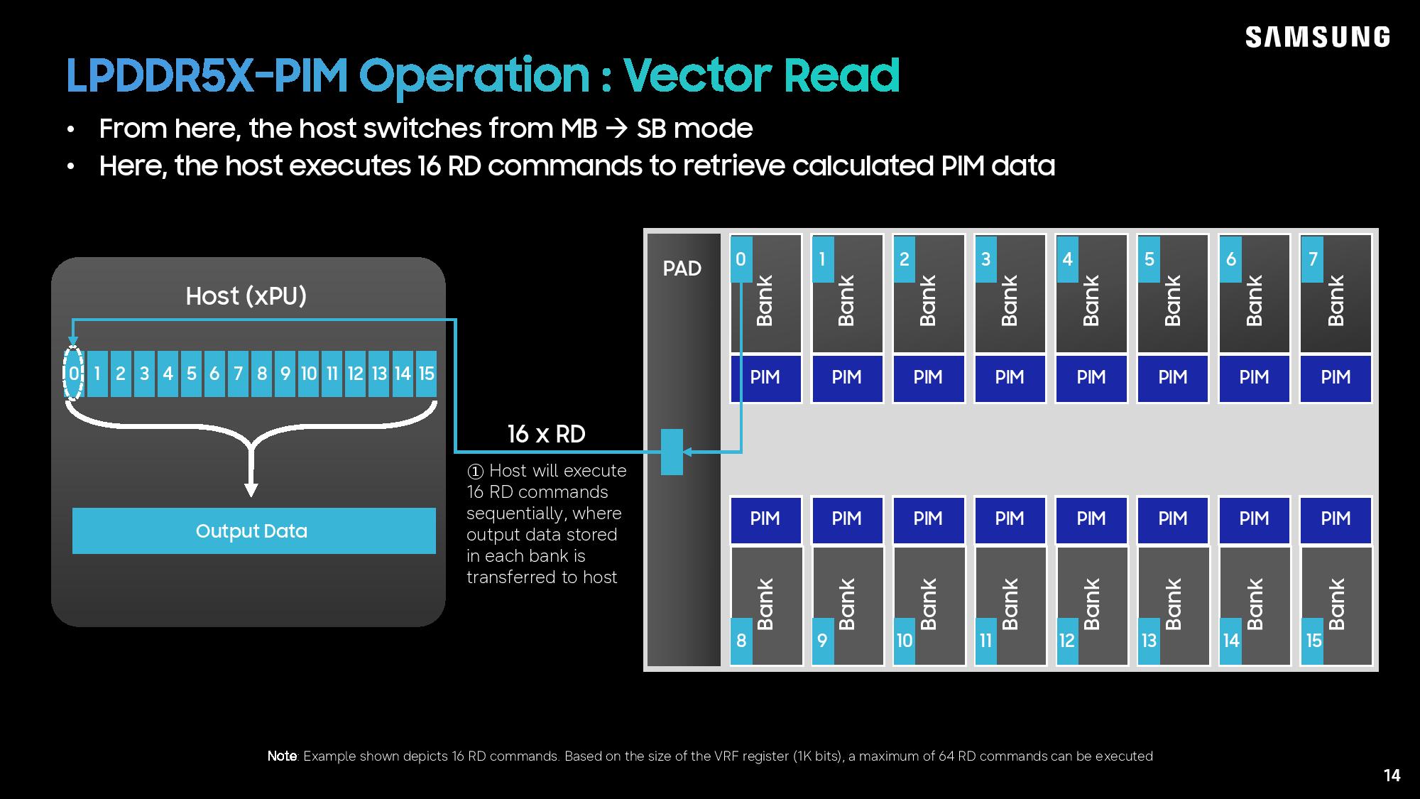
- Write-Back and Retrieval: A
PIMX_WRcommand transfers the processed data back into the main DRAM bank. The host system then briefly switches back to single-bank (conventional DRAM) mode, executing 16 rapid reads to gather the finalized outputs from all memory banks simultaneously.
Specifications, Performance Metrics, and Power Dynamics
Samsung’s physical implementation of LPDDR5X-PIM closely mirrors standard high-end memory modules, utilizing a familiar 561-ball array packaging grid configured across two 64-bit ranks on a 16GB module footprint (utilizing a total of eight dies, or four dies per rank).
Bandwidth Explosion
While a standard LPDDR5X-9600 module caps out at a respectable peak bandwidth of 76.8 GB/s, Samsung’s PIM-enabled architecture achieves an effective bandwidth equivalent of 614 GB/s—an astonishing eightfold increase. This massive leap is not achieved by raw bus-speed overclocking, but by completely eliminating the latency and bandwidth penalties of moving data back and forth across the physical trace lines to the host processor.
Benchmark Results
During internal testing utilizing Meta’s Llama 3.1 (8-billion parameter model) running on an advanced edge AI accelerator (widely suspected to be an early iteration of Samsung’s upcoming Gaia client SoC), the performance gains were undeniable:
- Model Run Time: Improved by 2.28x compared to standard, non-PIM LPDDR5X memory.
- Tokens Per Speed (TPS): Accelerated by 3.01x, drastically reducing time-to-first-token and streaming generation latency for generative AI applications.
The Power Consumption Paradox
One of the most pressing questions surrounding Processing-in-Memory is power efficiency. By adding active logic gates directly inside a low-power memory standard, does energy consumption skyrocket?
Samsung’s engineers tackled this head-on, admitting that peak power draw is significantly higher during active PIM execution phases due to the localized, bursty nature of the computational workload. However, looking at the macro picture, Samsung projects that overall power consumption will actually decrease compared to traditional DRAM architectures.
The rationale is simple mathematics: moving large blocks of data across high-speed external memory buses consumes massive amounts of electrical current. By processing data locally and drastically curtailing the frequency of data transit between the memory and the system processor, the energy saved on bus movement far outweighs the operational power cost of the onboard PIM logic. As Samsung presenter Karam Hwang succinctly noted during the Q&A session: "We’re not seeing a significant overall power increase."
Supporting Context: Industry Adoption and Shifting Paradigms
Historically, LPDDR memory variants were strictly confined to smartphones, tablets, and ultra-portable laptops due to thermal and form-factor constraints. However, the hardware ecosystem is rapidly evolving.
Recent architectural shifts have seen high-performance system designers breaking traditional boundaries:
- NVIDIA has embraced LPDDR5X via CAMM2 (Compression Attached Memory Module) serviceable modules, pairing the efficient memory standard with its powerful Vera CPU architectures.
- Intel has integrated LPDDR5X support into its newly unveiled Crescent Island AI accelerator, leveraging deep XMX compute engines alongside dense, low-power memory pools to maximize AI FLOPs-per-watt efficiency.
By expanding its target deployment scope across servers, client PCs, and mobile edge devices, Samsung is positioning LPDDR5X-PIM as the ultimate bridge technology. It provides a cost-effective, high-bandwidth alternative to HBM for secondary accelerators, while simultaneously unlocking local generative AI capabilities for everyday smartphones and laptops.
Future Outlook and Market Implications
Samsung’s successful hardware validation of LPDDR5X-PIM at Hot Chips 2026 marks a watershed moment for the semiconductor industry. As edge devices increasingly take on heavy AI workloads—running local language models, real-time computer vision, and autonomous agent tasks without relying on cloud-based server farms—the traditional memory bottleneck has become the ultimate enemy of progress.
Looking further ahead, Samsung has already set its sights on the next frontier: LPDDR6X-PIM. The company confirmed it is actively working with industry standardization bodies, expressing high hopes of securing an initial PIM specification from JEDEC within the calendar year.
While minor hurdles remain—such as ongoing algorithmic optimizations to ensure exact parity in model output accuracy without compromising inference speed—the writing is on the wall. Processing-in-Memory is no longer an academic curiosity or a hyper-niche enterprise luxury. With LPDDR5X-PIM, Samsung has proven that the future of AI acceleration lies not in building faster processors to fight the memory wall, but in turning the memory itself into the computer.