
SK Hynix Pushes Hybrid Bonding Out to HBM5, Citing Physical and Thermal Realities in AI Memory Packaging
Executive Overview
The semiconductor industry’s anticipated transition to copper-to-copper hybrid bonding for High Bandwidth Memory (HBM) has hit another roadblock. During a presentation at the Hot Chips 2026 conference, Jaesik Lee, Vice President of Package Engineering at SK Hynix America, clarified that the memory giant does not expect hybrid bonding to be production-ready for the upcoming HBM4E standard. Instead, this transformative packaging technique has been pushed out to HBM5 at the earliest.
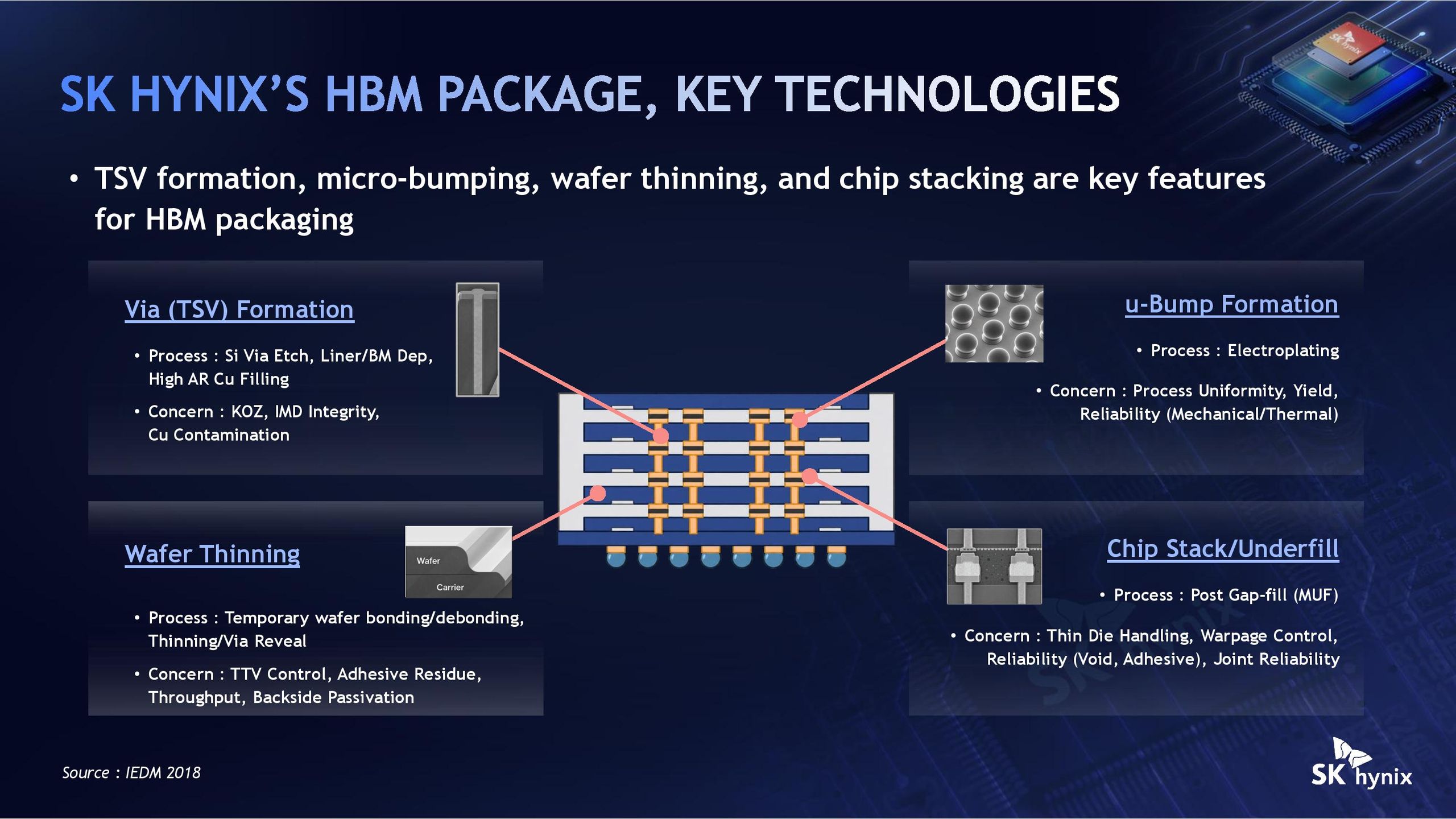
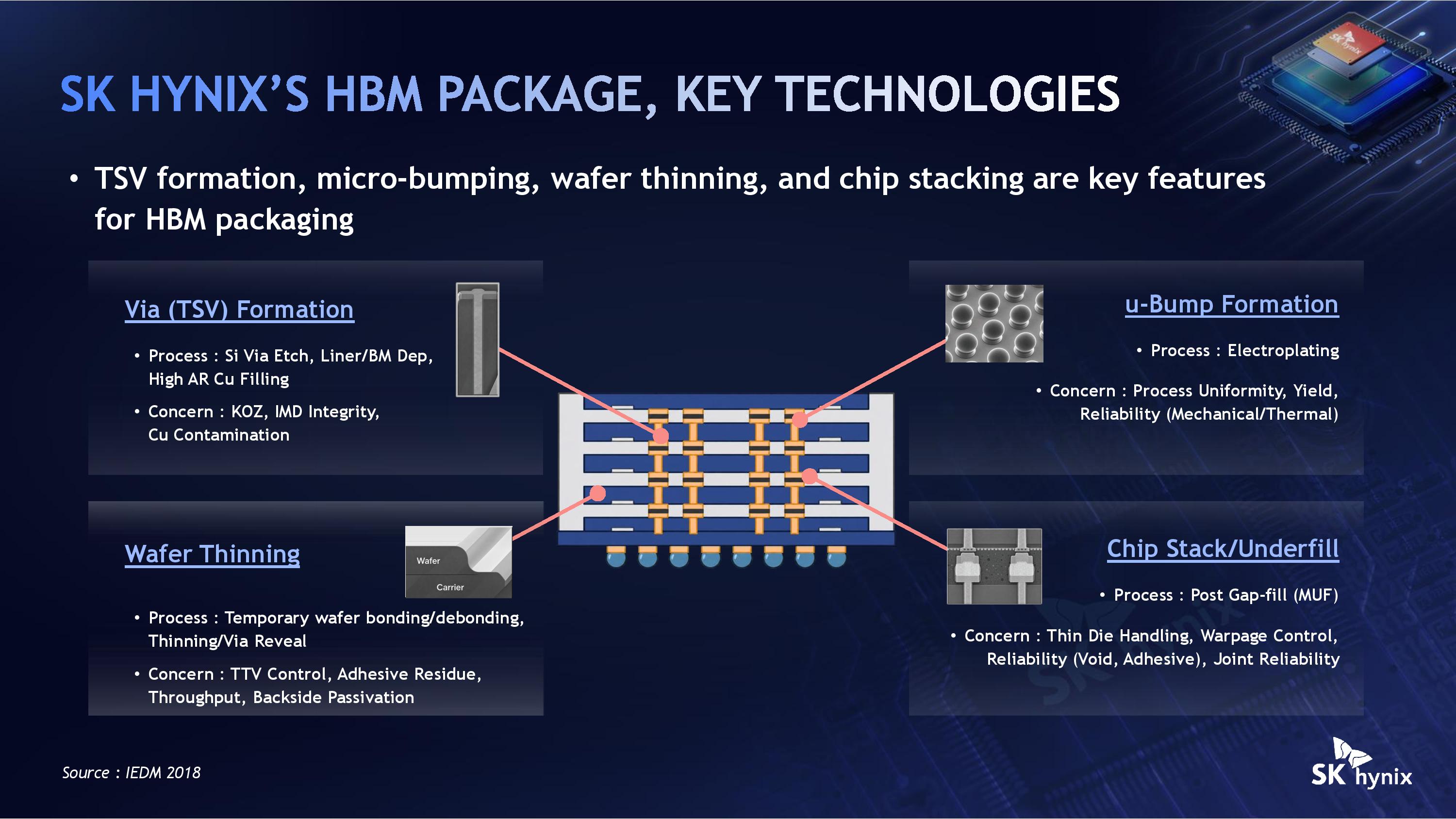
While rival manufacturers like Samsung have aggressively signaled intentions to adopt hybrid bonding earlier in the roadmap, SK Hynix continues to lean on its proprietary Mass Reflow-Molded Underfill (MR-MUF) process. According to SK Hynix, recent modifications to the JEDEC thickness ceilings—along with the staggering manufacturing complexities of aligning sub-50-micron, multi-layer die stacks—have bought MR-MUF an extended lease on life.
This deep dive examines the engineering barriers governing HBM development, the physics of the 775-micron stack limit, the thermal challenges of next-generation AI memory, and the broader architectural shifts reshaping the landscape of high-performance computing (HPC) memory.
Detailed Chronology: The Evolution of HBM Packaging Roadmaps
To understand why hybrid bonding has repeatedly slipped from near-term deployment schedules, it is necessary to examine the timeline of high-density memory packaging over the past few years:
- May 2024: Samsung publicly commits to implementing hybrid bonding for its HBM4 memory generation, setting a high benchmark for industry adoption and putting pressure on competitors to accelerate their copper-to-copper bonding R&D.
- Early 2025 – March 2026: Industry sources report that SK Hynix places its inaugural mass-production hybrid bonding order—a single inline tool system pairing Applied Materials and Besi technologies valued at approximately 20 billion won ($15 million USD). Concurrently, market research firms like Counterpoint Research project that hybrid bonding will enter full-scale HBM manufacturing by the HBM5 window (around 2029 to 2030).
- March 2026: Industry discussions emerge regarding a potential expansion of the JEDEC HBM thickness specification to 825–900 microns to accommodate burgeoning 20-Hi (20-layer) stacks. This relaxation of vertical constraints further diminishes the immediate pressure to transition to hybrid bonding.
- May 2026: SK Hynix publicly unveils its innovative iHBM (Integrated HBM) thermal architecture, designed to embed micro-cooling blocks directly inside the base die’s interface to target next-generation accelerators.
- August 23, 2026 (Hot Chips 2026): Jaesik Lee officially confirms during his keynote that hybrid bonding will miss the HBM4 and HBM4E windows, cementing MR-MUF as the primary vehicle for current high-capacity AI memory modules, such as the 48GB 16-Hi HBM4 stack currently undergoing customer qualification.
Supporting Context & Metrics: The Physics of the 775-Micron Limit
The core bottleneck in modern HBM design is not simply laying down copper connections; it is managing three-dimensional physical constraints governed by semiconductor manufacturing limits.
The 775-Micron Ceiling
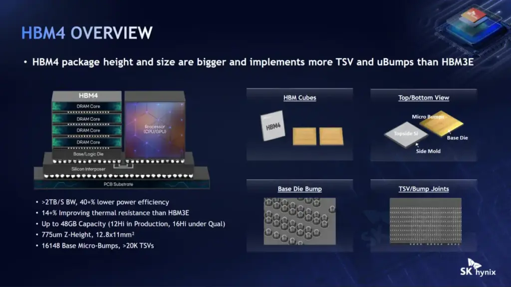
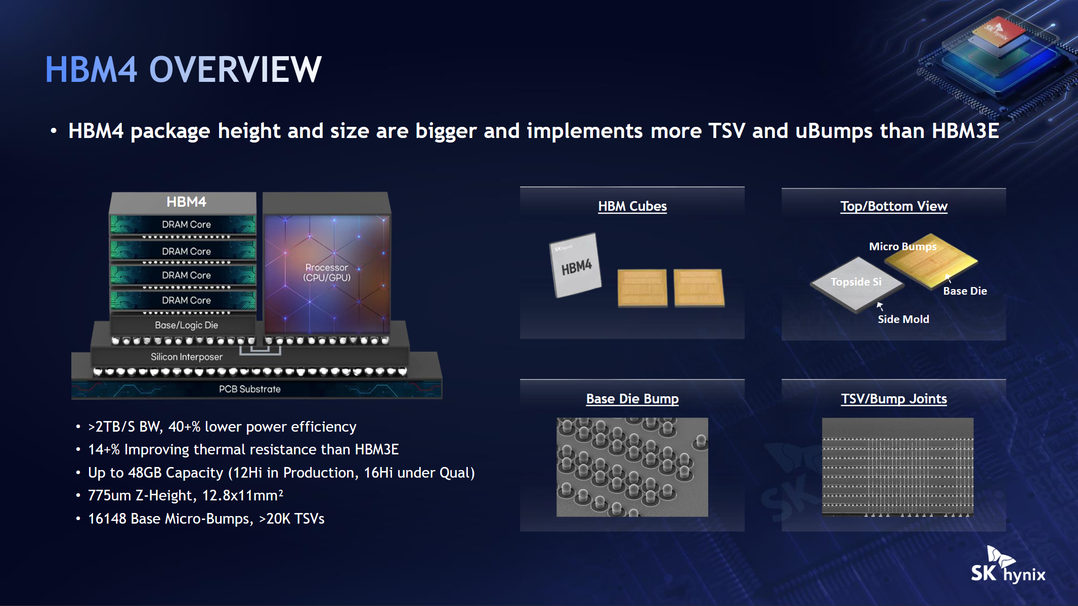
Under the JEDEC HBM4 standard, the total package thickness ceiling was raised from the 720-micron limit that defined the HBM3E era up to 775 microns. This relaxation provided critical relief for packaging engineers.
When a GPU or AI accelerator package undergoes final assembly, its cold plate is attached directly to the silicon. To ensure a flat, uniform thermal interface, both the underlying logic die and the adjacent memory stacks are ground down to expose bare silicon. Because standard 300mm logic wafers measure 775 microns in thickness, any memory cube that exceeds this height would stand proud of the processor beside it, catastrophic for cold plate seating and thermal conductivity.
As Jaesik Lee bluntly noted during his Hot Chips presentation:
"That’s the kind of limit that we can go up so far, because the logic wafer thickness is also 775 microns."
Thermal Resistance and Material Trade-offs
As memory stacks scale vertically to 12-Hi, 16-Hi, and eventually 20-Hi configurations, core DRAM dies must be aggressively thinned. For instance, 16-Hi HBM4 thins its core dies down to roughly 50 microns while halving the vertical gap between layers compared to 12-Hi equivalents.
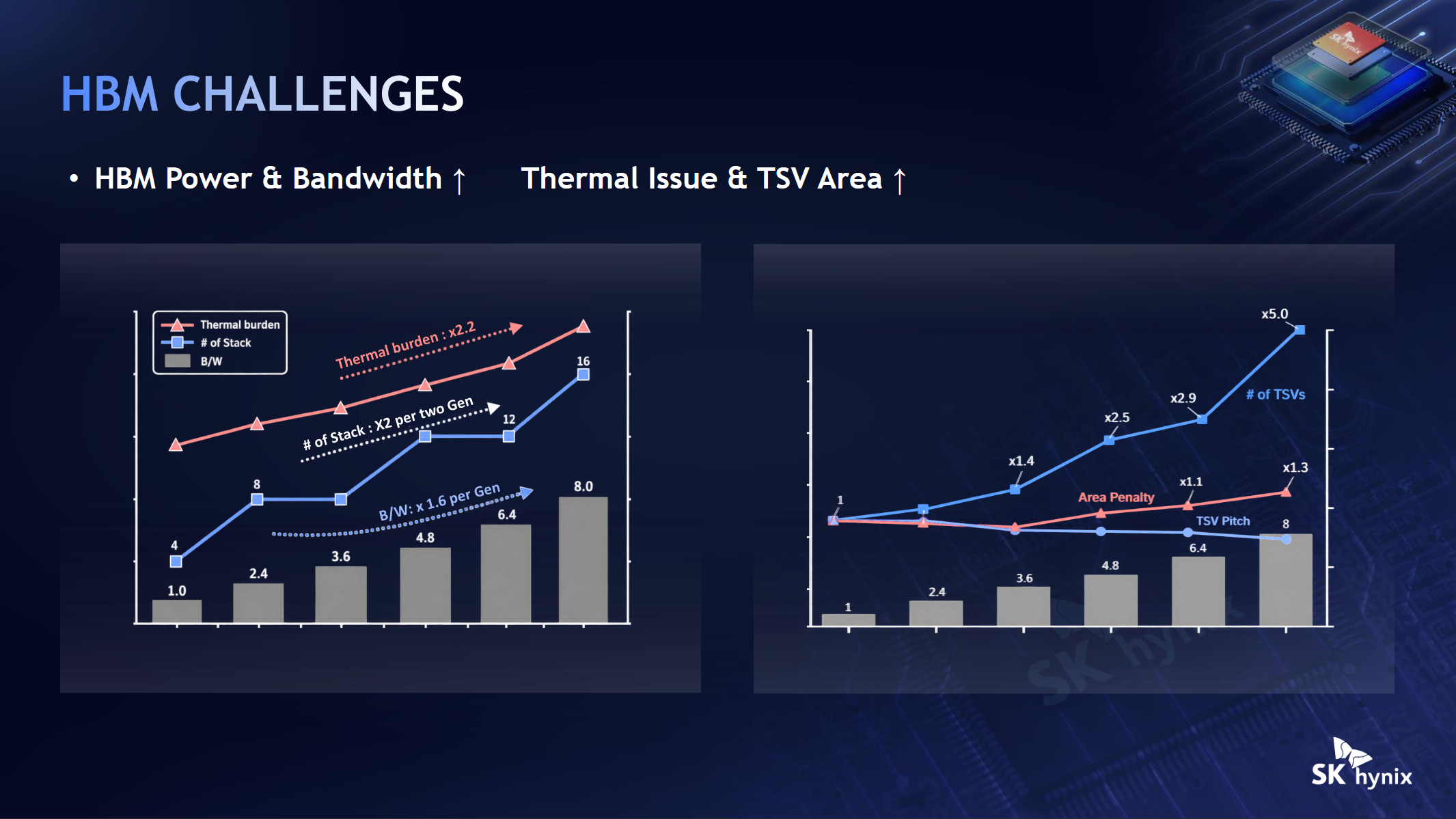
However, this structural thinning introduces a major thermal penalty. Thinner dies leave the stack with proportionally more oxide layers, which conduct heat significantly worse than pure silicon. Compounding this issue, pin speeds have skyrocketed from a modest 1 Gbps in early HBM iterations up to 8 Gbps in HBM4 (with 16-Hi HBM4 achieving speeds up to 10 GT/s over a 2,048-bit interface). This exponential increase in data transfer rates packs vastly more thermal energy into the exact same physical footprint.
SK Hynix’s internal metrics reveal that the thermal burden across successive HBM generations has surged by a factor of 2.2, while stack counts double every two generations. Managing these thermal densities without micro-bumps is precisely why advanced cooling architectures have become mandatory.
Official Statements and Technical Insights
The Case for MR-MUF and Why Hybrid Bonding Keeps Slipping
Despite its long-term promise, hybrid bonding—which joins flattened copper pads and oxide surfaces at room temperature before relying on thermal expansion during a cure step—is extraordinarily complex when applied to multi-layer stacks.
"This is a very simple process, but in reality it’s really challenging," Lee explained. "We are talking about 16 layers and 20 layers that we need to make the hybrid bonding, so it’s very different from the one-layer stacking."
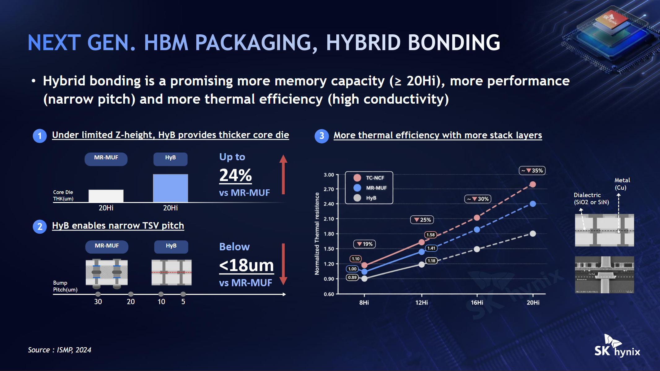
By eliminating micro-bumps entirely, hybrid bonding would allow core dies to grow up to 24% thicker in a 20-Hi configuration, cut thermal resistance by approximately 35% compared to MR-MUF, and shrink bump pitch to below 18 microns (down from the roughly 30-micron pitch standard in modern MR-MUF).
Yet, because the JEDEC thickness relaxation successfully accommodated HBM4, conventional micro-bumps remain entirely viable. SK Hynix’s Mass Reflow-Molded Underfill process—which stacks all dies via pick-and-place and joins them in a single reflow—remains scalable for now, even if filling shrinking gaps and managing warpage on sub-50-micron dies represents a formidable manufacturing hurdle.
The iHBM Thermal Architecture
To combat rising thermal loads, SK Hynix showcased further details regarding its iHBM thermal architecture. This innovation embeds thermally conductive, electrically insulating blocks directly into the base die’s die-to-die (D2D) PHY region—the exact interface hotspot where power density peaks.
According to company benchmarks, iHBM achieves a thermal resistance reduction of over 30%. However, Lee issued a strict design caveat: these thermal blocks cannot be retrofitted into any HBM generation already in the design pipeline. Because the blocks sit internally alongside the D2D PHY, they require meticulous co-optimization with the customer’s custom silicon design. Consequently, iHBM—much like competing solutions such as Samsung’s Heat Path Block approach and Micron’s base-die circuit redesign—is slated strictly for HBM5-class accelerators and dense AI data centers expected around 2028.
Future Outlook: Architectural Splits and Tiered Memory
During the vibrant Q&A session at Hot Chips 2026, Tanj Bennett of SemiAnalysis raised a critical architectural question: as memory stacks grow taller (such as 20-Hi configurations), does the average throughput of the stack degrade relative to the massive manufacturing capacity required? Bennett noted that native DRAM operating at the cell level can deliver upwards of 20 TB/s per square centimeter, whereas a towering 20-Hi stack tops out around 4 TB/s—making high-stack HBM theoretically slower in raw terms than alternative memory topologies like DDR5, while consuming disproportionate fab capacity.
Lee countered that modern AI training workloads demand an uncompromising blend of raw bandwidth and massive capacity. However, he conceded that future AI inference workloads may well fracture this paradigm, separating the active KV (Key-Value) cache inside high-bandwidth memory while offloading bulk storage to cheaper, more distributed LPDDR or high-capacity flash tiers.
This tiered memory approach is already transitioning from theory to silicon. Nvidia’s Vera Rubin architecture, for example, pools LPDDR5X with HBM4 over NVLink-C2C interconnects. Similarly, the High Bandwidth Flash (HBF) specification co-developed by SK Hynix and SanDisk extends this exact tiering philosophy directly into NAND storage structures, promising up to 3 TB/s of bandwidth via UCIe integration.
With SK Hynix commanding an estimated 70% of Nvidia’s HBM orders for the upcoming Vera Rubin generation—all of which will rely on tried-and-true MR-MUF packaging—the memory giant is in a commanding commercial position. While hybrid bonding and iHBM cooling remain the definitive future of memory packaging, their deployment will wait for HBM5, proving that in the high-stakes world of semiconductor manufacturing, evolutionary reliability frequently triumphs over revolutionary haste.